Getting started
Let us explore QEDA capabilities by creating a simple PCB. This will be an abstract Wi-Fi adapter which uses ESP-07 module.
We will use Ubuntu during demonstration but one may repeat following steps on any compatible operating system (with minor modifications).
Prerequisites
Be sure to have Node.js installed. Good command to check it is:
node --version
You should see something like this:
v7.3.0
If there is only nodejs command instead of node in your distribution you have to create symlink:
sudo ln -s `which nodejs` /usr/bin/node
Also fresh version of KiCad EDA should be installed.
Installation
The simplest way to install QEDA tools is to use NPM:
sudo npm install -g qeda
Verify whether installation completed successfully. Run:
qeda --version
If you see something like ...
QEDA v0.2.11... we can continue.
Create directory for our future PCB project:
mkdir wifi-adapter
cd wifi-adapter
Step 1: Apply manufacturer's design rules
Any PCB manufacturer has some limitations specified by production capabilities.
For example let's explore OSH Park guidelines:
- 6 mil (0.2 mm) minimum spacing
- 13 mil (0.4 mm) minimum drill size
- 7 mil (0.2 mm) minimum annular ring
Create subdirectory for elements library:
mkdir lib
cd lib
And apply these restrictions (all dimensions are in millimeters):
qeda config pattern.clearance.padToPad 0.2
qeda config pattern.minimum.drillDiameter 0.4
qeda config pattern.minimum.ringWidth 0.2
Please refer to Command-line utility section for details about all options available.
After executing commands above there will be new .qeda.yaml file with correspondent settings. This file will contain data produced by qeda command.
Step 2: Other settings
We can choose preferred method of land pattern generation: using recommended dimensions provided by element manufacturer or using IPC-7351 standard. This method is controlled by pattern.preferManufacturer configuration parameter and has true value by default.
IPC-7351 standard provides three component density levels:
- Minimum (Least,
L) Land Protrusion — high component density typical of portable and hand-held product applications. - Median (Nominal,
N) Land Protrusion — products with a moderate level of component density. - Maximum (Most,
M) Land Protrusion — for low-density product applications.
We do not care about free space so we will choose lowest (M) density level:
qeda config pattern.densityLevel M
Our future PCB assumed to be manually soldered therefore another parameter should be set: minimal distance from lead end to correspondent pad edge:
qeda config pattern.minimum.spaceForIron 0.5
Step 3: Adding elements
Elements used are already in repository so we need only to add them:
qeda add module/esp-07
qeda add capacitor/c0603
qeda add capacitor/c1210
qeda add resistor/r0603
qeda add misc/tp-th-1
qeda add ti/lm1117mpx
qeda add hirose/df13a-6p-1.25h
You may examine their definitions if you are interested in:
- Module ESP-07
- Capacitor C0603
- Capacitor C1210
- Resistor R0603
- Misc TP-TH-1
- TI LM1117MPX
- Hirose DF13A-6P-1.25H
If there is no element needed in repository you can add new one. Please refer to Component description section for details.
Some power and ground symbols are to be added too:
qeda power +5V
qeda power +3V3
qeda ground signal/GND
Step 4: Library generation
This step is quite easy. Let's call our library wa:
qeda generate wa
You will see many lines of text that should end with KiCad libraries files generation:
Generate output for 'wa'
  KiCad library 'wa.lib'
  KiCad library doc 'wa.dcm'
  KiCad footprint 'SON200P2120X1600X300-16M.kicad_mod'
  KiCad footprint 'CAPC1608X92M.kicad_mod'
  KiCad footprint 'CAPC3225X230M.kicad_mod'
  KiCad footprint 'RESC1608X55M.kicad_mod'
  KiCad footprint 'TP-TH-1.kicad_mod'
  KiCad footprint 'SOT230P700X180-4M.kicad_mod'
  KiCad footprint 'HIROSE_DF13A-6P-1.25H.kicad_mod'
Now we have two new subdirectories:
librarycontaining cached YAML-descriptions of used elementskicadwith library files intended to be used in KiCad
Step 5: Schematic design
Create new KiCad project in wifi-adapter/board directory.
As our new library is all-sufficient one may delete any others libraries provided by Kicad by default.
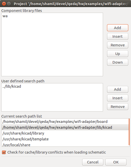
Using wa library add new elements and complete the schematic.
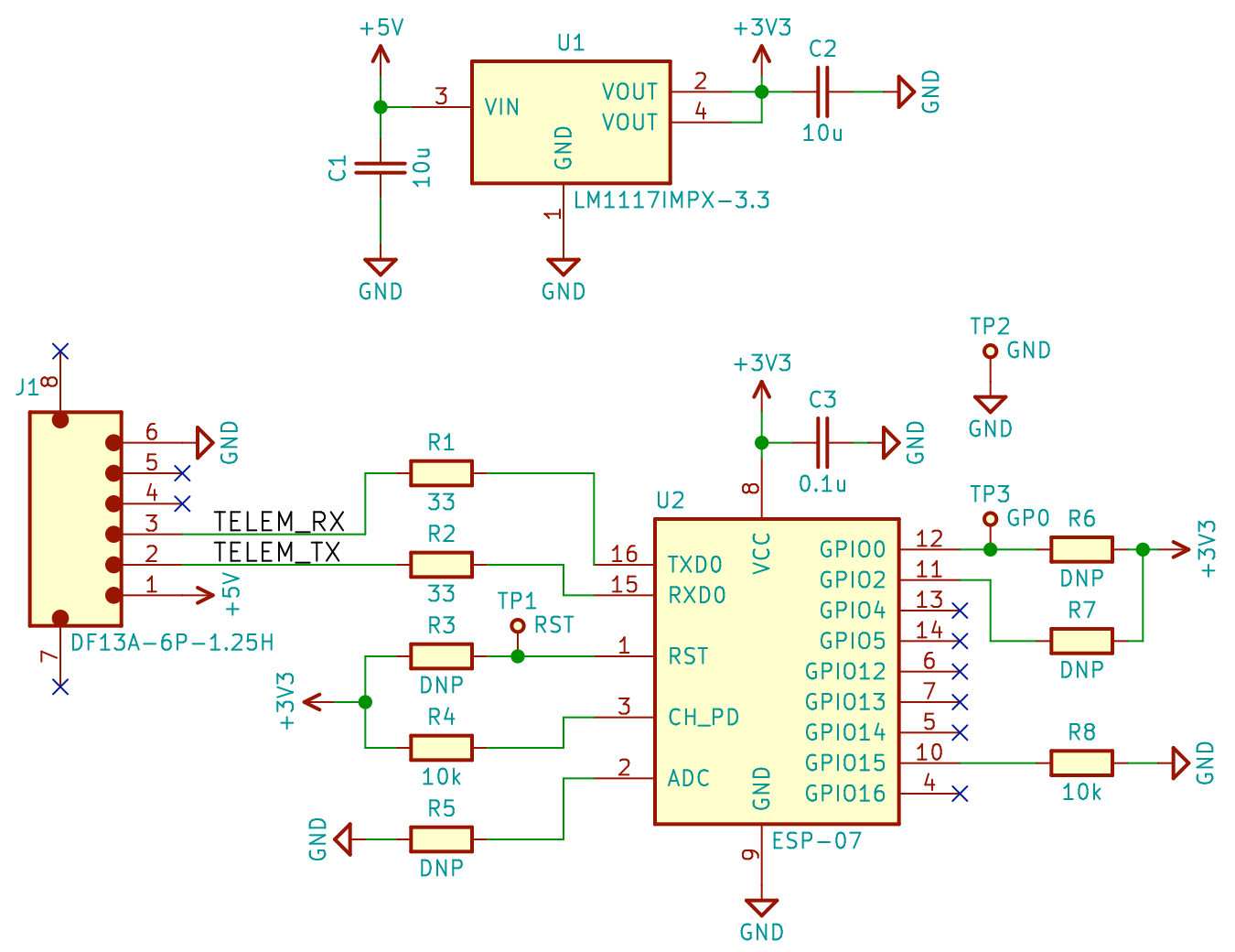
There is a good news! With our library generated by QEDA we do not need to run KiCad's Cvpcb in order to assign component footprints. All schematic symbols already have their own land patterns assigned.
After generating netlist we are ready for the next final step.
Step 6: PCB Routing
Firstly we are to inform PCB editor to get land patterns from our wa library. In order to do it we create fp-lib-table file in project directory and fill it with text:
(fp_lib_table
  (lib (name wa)(type KiCad)(uri ${KIPRJMOD}/../lib/kicad/wa.pretty)(options "")(descr ""))
)
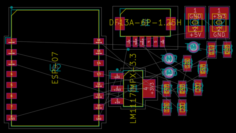
Import netlist then perform auto spread.
Complete PCB routing.
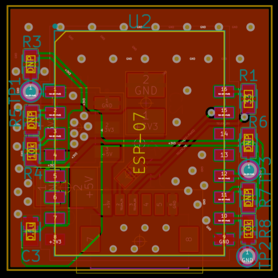
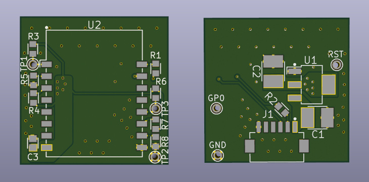
Now we can generate gerber files and make an order of our new PCB.
That's all!
Source files
GitHub: https://github.com/qeda/examples/tree/master/wifi-adapter
 QEDA Documentation